


Please Leave Us A Message
Privacy statement: Your privacy is very important to Us. Our company promises not to disclose your personal information to any external company with out your explicit permission.
 Mr. John chang
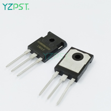
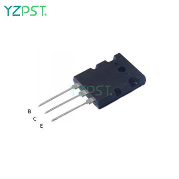
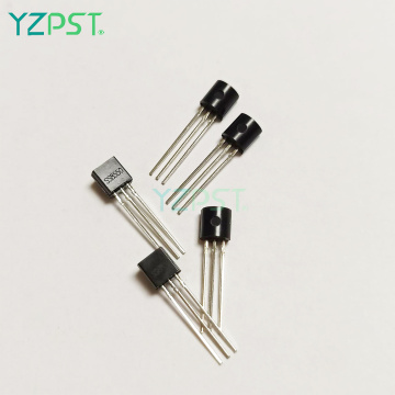
Model No.: YZPST-SS044N10AP
Brand: YZPST
Application: Microphone, Not Applicable
Supply Type: Original Manufacturer
Reference Materials: Datasheet, Photo
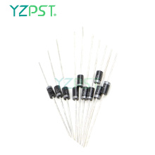
Package Type: Surface Mount
Installation Method: Not Applicable
FET Function: Not Applicable
Configuration: Not Applicable
VDSS: 100V
ID: 135A
IDM: 520A
VGSS: ±20V
EAS: 780mJ
PD: 208W
Packaging: 1. Anti-electrostatic packaging 2. Carton box 3. braid
Productivity: 1000000000
Transportation: Ocean,Land,Express,Air
Place of Origin: CHINA
Supply Ability: 1000000000
Port: SHANGHAI
Payment Type: L/C,T/T,Paypal
Incoterm: FOB,CFR,CIF

| Device Ordering Marking Packing Information | |||
| Ordering Number | Package | Marking | Packing |
|
SS044N10AP |
TO-220 | YZPST SS044N10AP |
Tube |
| Absolute Maximum Ratings TC = 25ºC, unless otherwise noted | |||
|
Parameter |
Symbol | Value |
Unit |
| TO-220 | |||
| Drain-Source Voltage (VGS = 0V) | VDSS | 100 | V |
| Continuous Drain Current | ID | 135 | A |
| Pulsed Drain Current (note1) | IDM | 520 | A |
| Gate-Source Voltage | VGSS | ±20 | V |
| Single Pulse Avalanche Energy (note2) | EAS | 780 | mJ |
| Power Dissipation (TC = 25ºC) | PD | 208 | W |
| Operating Junction and Storage Temperature Range | TJ, Tstg | -55~+150 | ºC |
| Caution: Stresses greater than those listed in the “Absolute Maximum Ratings” may cause permanent damage to the device. | |||
| Thermal Resistance | |||
|
Parameter |
Symbol | Value |
Unit |
| TO-220 | |||
| Thermal Resistance, Junction-to-Case | RthJC | 0.60 | ºC/W |
| Thermal Resistance, Junction-to-Ambient | RthJA | 62.5 | |
| Specifications TJ = 25ºC, unless otherwise noted | ||||||
|
Parameter |
Symbol |
Test Conditions | Value |
Unit | ||
| Min. | Typ. | Max. | ||||
| Static | ||||||
| Drain-Source Breakdown Voltage | V(BR)DSS | VGS = 0V, ID = 250µA | 100 | -- | -- | V |
| Zero Gate Voltage Drain Current | IDSS | VDS =100, VGS = 0V, TJ = 25ºC | -- | -- | 1.0 | μA |
| Gate-Source Leakage | IGSS | VGS = ±20V | -- | -- | ±100 | nA |
| Gate-Source Threshold Voltage | VGS(th) | VDS = 250µA | 2.0 | -- | 4.0 | V |
| Drain-Source On-Resistance (Note3) | RDS(on) | VGS = 10V, ID =50A | -- | 3.6 | 4.4 | mΩ |
| Dynamic | ||||||
| Input Capacitance | Ciss |
VGS = 0V, VDS = 50V, f = 1.0MHz | -- | 7300 | -- |
pF |
| Output Capacitance | Coss | -- | 850 | -- | ||
| Reverse Transfer Capacitance | Crss | -- | 25 | -- | ||
| Total Gate Charge | Qg |
VDD = 50V, ID = 20A, VGS = 10V | -- | 114 | -- |
nC |
| Gate-Source Charge | Qgs | -- | 37 | -- | ||
| Gate-Drain Charge | Qgd | -- | 26 | -- | ||
| Turn-on Delay Time | td(on) |
VDD = 50V, ID =50A,VGS = 10V RG =3.0 Ω | -- | 32 | -- |
ns |
| Turn-on Rise Time | tr | -- | 50 | -- | ||
| Turn-off Delay Time | td(off) | -- | 83 | -- | ||
| Turn-off Fall Time | tf | -- | 30 | -- | ||
| Drain-Source Body Diode Characteristics | ||||||
| Continuous Body Diode Current | IS |
TC = 25 ºC | -- | -- | 135 |
A |
| Pulsed Diode Forward Current | ISM | -- | -- | 520 | ||
| Body Diode Voltage | VSD | TJ = 25ºC, ISD = 50A, VGS = 0V | -- | 0.9 | 1.2 | V |
| Reverse Recovery Time | trr | VGS = 0V,IS = 50A, diF/dt =500A /μs | -- | 75 | -- | ns |
| Reverse Recovery Charge | Qrr | -- | 160 | -- | nC | |
Notes
1. Repetitive Rating: Pulse width limited by maximum junction temperature
2. VDD = 50V, RG = 25 Ω , Starting TJ = 25 ºC
3. Pulse Test: Pulse width ≤ 300μs, Duty Cycle ≤ 1%
Product Categories : Semiconductor Plastic Package > Silicon Transistor


Privacy statement: Your privacy is very important to Us. Our company promises not to disclose your personal information to any external company with out your explicit permission.
Fill in more information so that we can get in touch with you faster
Privacy statement: Your privacy is very important to Us. Our company promises not to disclose your personal information to any external company with out your explicit permission.