


Please Leave Us A Message
Privacy statement: Your privacy is very important to Us. Our company promises not to disclose your personal information to any external company with out your explicit permission.
 Mr. John chang
 January 30, 2019
As shown in the figure, 555 and R1, RP1, C2, etc. constitute a trigger delay circuit. Normally, since R1 is connected to VDD, 555 is in the reset state, that is, the 3 pin is at a low level; when the trigger signal arrives, the SCR is turned on, and the 2 pin has a low level signal, so that the 555 is inverted and the output is high. The temporary stability width is τ=1.1RP1C2. After triggering, the SCR is turned off. This circuit reduces the need for trigger pulses. If the CMOS type 555 (or 556) is used, the trigger current can also be reduced.
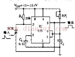
The above is the Trigger circuit controlled by thyristor based on 555 integrated chip we have listed for you. You can submit the following form to obtain more industry information we provide for you.
You can visit our website or contact us, and we will provide the latest consultation and solutions
Send Inquiry
Most Popular
lastest New
Send Inquiry


Privacy statement: Your privacy is very important to Us. Our company promises not to disclose your personal information to any external company with out your explicit permission.
Fill in more information so that we can get in touch with you faster
Privacy statement: Your privacy is very important to Us. Our company promises not to disclose your personal information to any external company with out your explicit permission.